My Programmable PSU rev 0.1 boards have been a great learning experience so far, which is exactly what I expected and hoped for. I’ve already accumulated a ton of lessons learned from the process and rev 0.2 will hopefully be a significant improvement and get me well down the path to the final product. Over the past couple of weeks I have watched a bunch of videos about PCB layout in general, and Kicad in particular and now feel much better informed and armed for tackling rev 0.2. Some of the key lessons learned so far are:
- Decoupling caps need to be right next to the IC
- Build logical groups of components (generally matching functional blocks in your schematic) and lay those out individually before bringing everything together as a whole.
- Use larger traces for power
- Use a copper fill if necessary to help with heat dissipation
- Get your crystal / oscillator as close to the micro-controller as possible. I found a great resource at http://hoani.net/engineering/crystal-oscillator-design/ for crystal oscillator design including PCB layout
- Be careful USB – it requires differential pairs that need to be carefully handled.
- If you can fit component values on your silkscreen – do it. It makes assembly a lot easier than having to constantly refer to a schematic to check values
Item #4 above relates to the LM317 regulator I am using to convert down from the 12v input to a 3.3v supply for the STM32. I am using the SOIC-8 package version of this device, and it gets hot. It has 4 output pins and I have only connected one of them. One thing I will definitely do next time is connect all four pins together with as large a copper fill as possible between the pins underneath the chip. This should go someway to helping with the heat dissipation.
I learned one particularly hard lesson about Kicad and making sure you re-draw the copper fills before generating your gerber files. You can read my debugging journey on this reddit thread. Once I had figured out what had gone wrong I tweeted about it and got some great advice back. Apparently this has been fixed in Kicad 5 where you can select an option to check zone fills before plotting – clearly I wasn’t the first person to be bitten by this issue!
Unfortunately though it resulted in a couple dead shorts on the board where VDD was connected directly to GND e.g.:
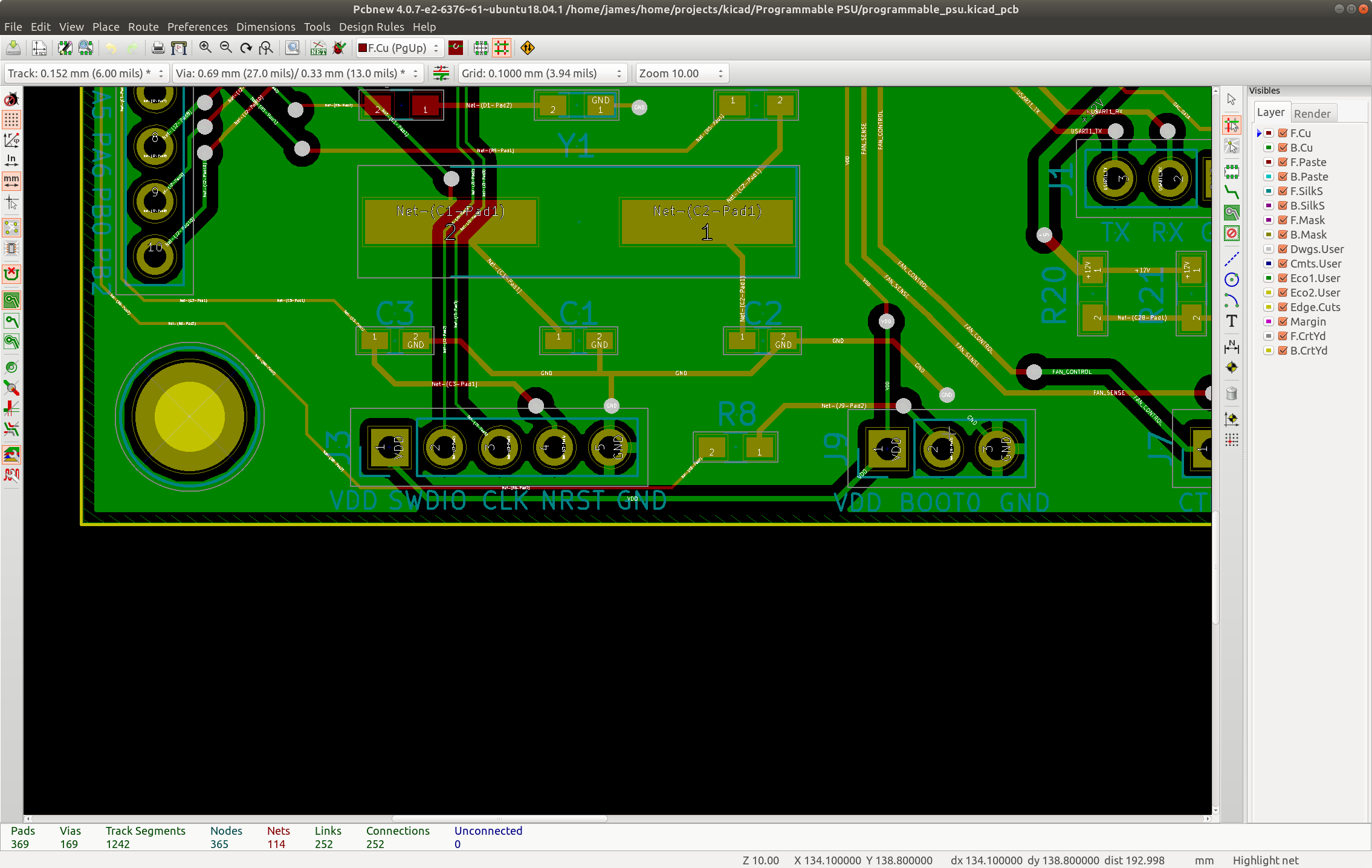
This is what I saw in pcbnew.
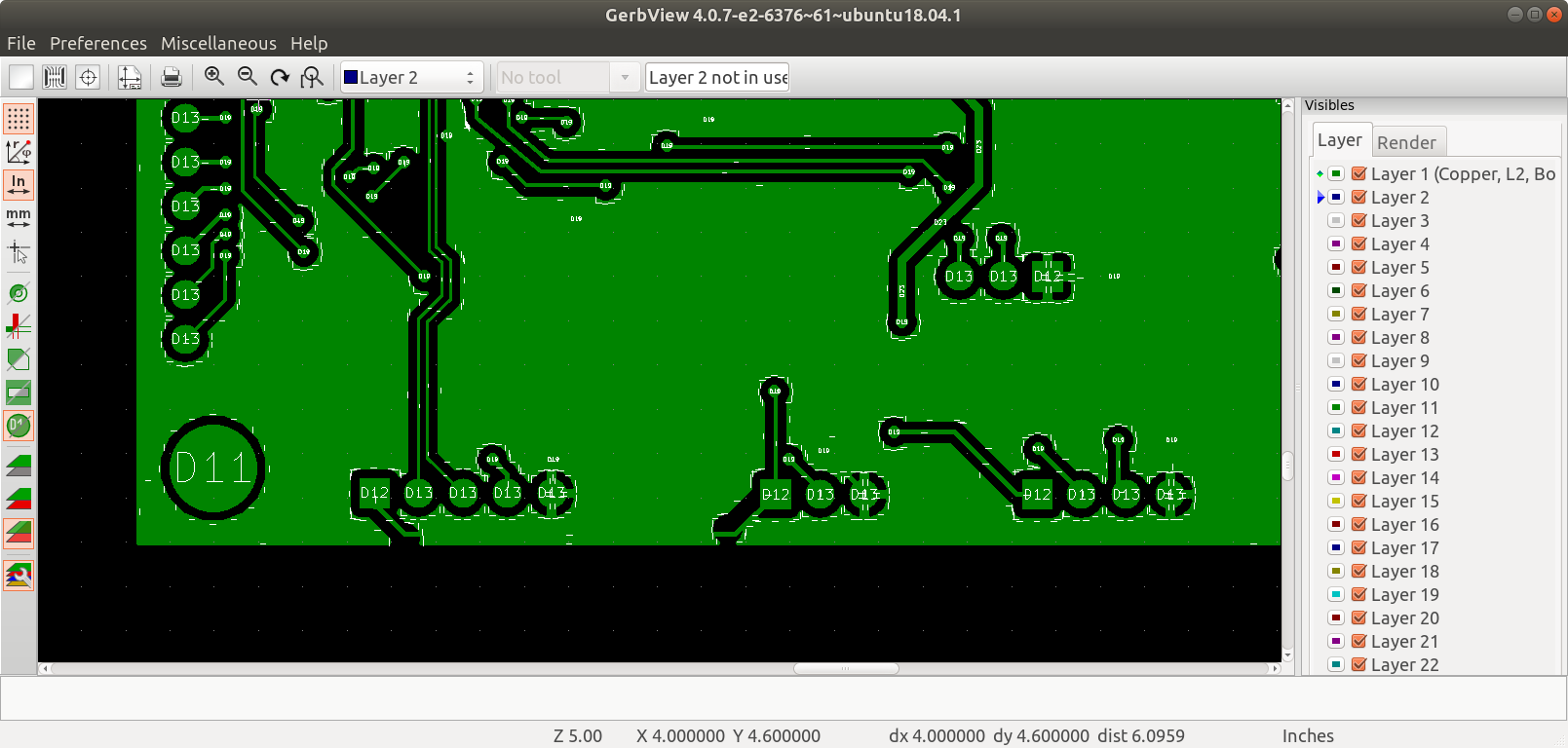
This is what the generated gerber file looks like.
Some judicious cuts with a craft knife and the boards are salvageable which is fortunate. Ultimately they were just intended to prove the digital control portion of the design using the STM32F070CBT6 which I should still be able to achieve with the rev 0.1 design.
After spending more time than I care to admit on figuring out the previous problem, I then had to diagnose why my STM32 kept hanging every time it got to the SystickHandler. Long story short I had jumpered BOOT0 to VDD instead of GND – won’t be making that mistake again either!
So, after all that I finally had a booting board and here is a blinky video to prove it:
