PSU Project Update 3

In my last PSU project update I mentioned that the software functions I still had to prototype were:

  • PWM control of the FAN (Intel FAN control spec)
  • Dithering of DAC output
  • Temperature reading

I now have the FAN control implemented and am working on the DAC dithering and temperature reading. I’ve started work on the DAC dithering, and I have now managed to convince myself of how that is going to work. Gerry described the general approach quite well in his post here, but writing an actual implementation of a driver to take a 18 bit number and simulate that output on a 16 bit DAC took a bit of thinking. I’ll detail that further in a future post once I have the software done.

I also now have the LM35 temperature sensors, so hopefully prototyping that final outstanding piece of functionality is just a matter of finding the time to read the data sheet and write a driver.

Intel Fan Driver

The Intel Fan driver turned out to be more interesting to write than I initially anticipated. The speed control aspect is pretty straight forward, and simply entails generating a 25kHz PWM output and varying the duty cycle. For my particular fan I found that even with a 0% duty cycle the fan has a minimum speed of 1000 RPM.

The tachometer part of the driver required a bit more thought. The specification dictates that the fan needs to output two pulses per revolution. I initially went down a bit of a blind alley with the idea that I could use the input capture function of the SMT32 Timers to calculate the number of pulses being received per second. That approach quickly became complicated and after some time away from the keyboard and giving it some more thought with a clear head I realised it was as simple as configuring an GPIO input pin to interrupt each pulse, keep a running total of the pulses in the interrupt routine, and then using the Timer to interrupt each second and calculate the actual speed of the fan and reset the current count.

The following photo shows the board running the fan with the oscilloscope displaying the output pulses from the fan:

Fan output pulse trace on scope

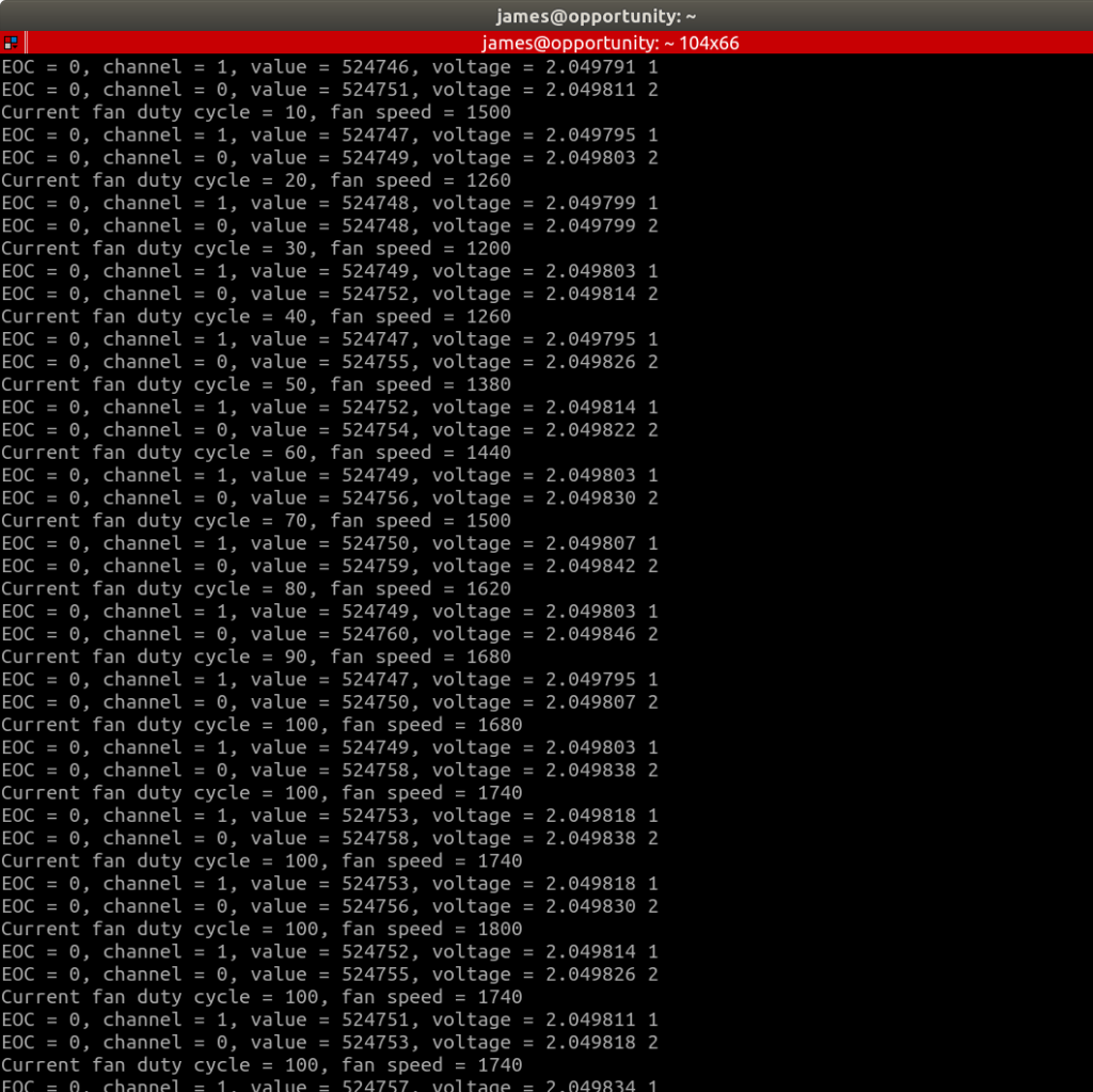
The current test software simply increments the output speed by 5% every seconds after the board starts up until it reaches 100%. The test program outputs the current fan speed to the UART each loop. The following screenshot shows the terminal output with the fan speed incrementing each loop (and the ADC reading back the current DAC output):

Console output showing fan speed

The software is using a fairly standard C driver approach. I have a struct which represents the hardware resources and state that needs to be tracked over time. This is the “fan” object. Then there are several functions that take a pointer to the fan struct and perform the functional operations such as calculating the current speed, or changing the output PWM to set the speed.

/*
 * fan.h
 *
 *  Created on: 25/07/2019
 *      Author: james
 *
 *  The Fan class provides a driver for an Intel 4 wire CPU cooling fan.
 *  This class depends on two interrupt functions in stm32f0xx_it.c for the GPIO interrupt
 *  on the FAN_SENSE pin, and the timer interrupt to calculate the fan speed.
 *  The fan generates 2 pulses per revolution. The GPIO interrupt simply counts the pulses. A
 *  Timer interrupt every 1000 milliseconds will call the UpdateSpeed function to calculate
 *  the current fan speed in RPM.
 */

#include "stdint.h"
#include "tim.h"

#ifndef FAN_FAN_H_
#define FAN_FAN_H_

// The state structure for the fan.
typedef struct {
	TIM_HandleTypeDef* pwm_handle;
	uint32_t pwm_channel;
	uint32_t tach_rpm;
	uint32_t tach_count;
} fan_t;

HAL_StatusTypeDef Fan_Init(fan_t* fan);
HAL_StatusTypeDef Fan_SetDutyCycle(fan_t* fan, int8_t percentage);
HAL_StatusTypeDef Fan_UpdateSpeed(fan_t* fan);
uint32_t Fan_GetSpeed(fan_t* fan);

#endif /* FAN_FAN_H_ */

I’m using the ST CubeMX software to do all the configuration of the STM32 and generate the framework code. I have read a lot of negative sentiment about the ST HAL libraries and, if I’m being honest, I can be a bit of a purest and so I can understand where this comes from. However, for someone who wants to get a project up and running with a limited amount of time available, the CubeMX software and HAL libraries make implementing functionality significantly quicker than if I was rolling my own firmware using bare bones register programming.
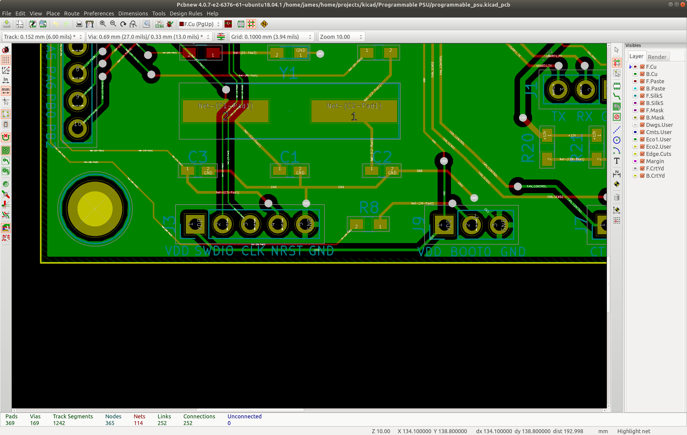
My one gripe though is that it does make your code quite fragmented. A good example of this is the timer configuration in the Fan driver.

When you configure peripherals using CubeMX it groups the configuration code for common peripherals together. You can also choose to have this code separated out into individual header and source files per peripheral. This is obviously better than everything being dumped in main.c, however it’s still not ideal, as when you are writing drivers your hardware configuration ends up being spread across different files with no obvious connection between them.

The only real solution to this appears to using the CubeMX software to do the initial configuration and code generation, but then move / refactor the generated code into your own driver files. Of course at this point you can no longer use the generate code function of CubeMX update the generated configuration. This of course is not ideal, but I think probably preferable to having functionality spread through a number of different source and header files. Time will tell….


PSU Project update 2

It’s been a long time since my last update as I have a large number of pressures on my time and I much prefer working on my projects to writing about them!

Some progress has been made, although slower than I would like. Since my last update I have completed the assembly of two prototype control boards. The second was required because during some rework on the first board I managed to lift some pads on the tiny MSOP-8 footprint for the ADC. These pads are really very small, and it is very easy to put just a fraction to much heat into them and lift them from the FR4.

As a result of assembling the two boards I have learnt a number of lessons and identified several improvements for the next revision. Some of key lessons learned have been:

  1. add test points for all important signals e.g. SPI lines
  2. orient all ICs in same direction
  3. add pin 1 indicator on silkscreen
  4. add component value on silkscreen
  5. Check, check and triple check the footprint matches the part you have ordered.

Point 5 above seems to be a common mistake, and all things considered I did pretty well for a first attempt. The footprint for my USBLC6-2SC6 was wrong, so USB will have to wait until the rev 2. board. One approach I have read of other people using to avoid these kinds of mistakes is printing the PCB one to one scale and laying the physical parts out on top to double check the footprints. I might try this before I send out my next board for manufacturing.

Firmware:

I’ve made good progress with the firmware development and have prototype code for the following functions:

  • Setting an output voltage using the DAC
  • Read back of the output voltage using the external ADC
  • Monitoring of the input voltage using the MCU ADC
  • Serial protocol for UART / USB interface
  • Rotary encoder reading for user input
  • ILI9341 320×240 TFT LCD display for user interface

Functions I have still to start are:

  • PWM control of the FAN (Intel FAN control spec)
  • Dithering of DAC output
  • Temperature reading

User interface:

The user interface has been an interesting challenge. To simplify the hardware in order to be able to focus just on the software I decided to use a temporary test platform using a “bluepill” development board which is a cheap STM32F103C8 based board available from Aliexpress for just a few dollars.

These little modules are really handy for mocking thing up on a breadboard and the STM32F103C8 is close enough to the STM32F070CBT6 part on my PSU controller that there is virtually no work required to port the code after prototyping. Here’s a picture of my prototype lashup with the ILI9341 TFT and rotary encoder attached.

Temporary UI development platform

The rotary encoder is the only UI input device at the moment. I may swap the TFT for a touch screen later depending how how this prototype goes, but navigating about using just the rotary encoder seems to work well enough for now.

The UI is based on a simple state machine. The user uses the rotary encoder to scroll through the various options VSET -> VCTRL -> CSET -> CCTRL, and uses the push button function on the encoder to select an option. They can then set the required voltage output in VSET state, or current output in CSET state. The encoder driver has “velocity control” built into it, so slow turns will increment the voltage in millivolt steps, slightly faster turns in 100mv steps and very fast turns in 1v steps, and similarly for the current control function.

Here is a short video of the UI in action:

Prototype PSU User Interface

As you can see I still have some issues to resolve with the fonts. Getting nice fonts to work was a challenge requiring reducing font files down to just the font sizes, and even characters I need to save space.

Final steps with the UI for now will be to integrate that code back into the main PSU firmware project, and figure out which SPI device – DAC or ADC – makes the most sense to share a SPI bus with the TFT screen.

PSU Project Update

It’s been a while since my last update on this project. This has largely been due to a month or so of big weeks at work delivering to a project deadline, and lots of family commitments in my personal time. Work is returning to normal now, so I’m hoping to sneak in a bit of progress on this and another couple of projects before the Christmas madness hits.

I’ve pretty much finished the board assembly now. I’ve just been waiting on the replacement 74HC4053 chips as I had mistakenly ordered SOIC wide i.e. 7.9mm wide instead of the standard 3.9mm  wide SOIC in my first digikey order  – doh!

Putting together this last Digikey order was a huge task. I feel like I need to find a better process / workflow for managing my BOM. It was quite a complicated process to keep track of what parts I need, for this revision, vs what was in the original BOM, minus what I have in stock… There must be an easier way than the spreadsheet/filter nightmare I’ve just been through so if anyone has suggestions please let me know!

Here is the board in it’s current state:

Mostly assembled board

I have a bunch of firmware development tasks I can work on with this revision:

  • PWM control of the FAN (Intel FAN control spec)
  • Dithering of DAC output
  • Read back of the output voltage using the external ADC
  • Monitoring of the input voltage using the MCU ADC
  • Temperature reading
  • Serial protocol for UART / USB interface
  • Rotary encoder reading for user input
  • ILI9341 320×240 TFT LCD display for user interface

Hopefully I should be able to get the bulk of of the firmware development done with the rev 0.1 board.  In parallel I’m going to start laying out rev 0.2 which will include the full regulator for the low voltage (8V at up to 8A) version.

I had initially thought that I may have to do a couple of prototypes of just the digital control portion before I started on the full board including the analog regulator circuit. However, I now think I may be able to get away with just the one version. Time will tell once I have got further into the firmware development.

One thing I have now realised is that I have messed up some of the pin allocations for the STM32 in rev 0.1 as some of the functions have conflicts. Hopefully I’ll be able to move some of the allocations around a bit and be able to stick with the STM32F070CBT6 part and not have to move up to a higher pin count device. I have a few unallocated pins to play with and  could potentially move the DAC and ADC to the same SPI master if I need to recover more, so I have some ideas about how to tackle this issue.


Lessons learned in PCB layout

My Programmable PSU rev 0.1 boards have been a great learning experience so far, which is exactly what I expected and hoped for. I’ve already accumulated a ton of lessons learned from the process and rev 0.2 will hopefully be a significant improvement and get me well down the path to the final product. Over the past couple of weeks I have watched a bunch of videos about PCB layout in general, and Kicad in particular and now feel much better informed and armed for tackling rev 0.2. Some of the key lessons learned so far are:

  1. Decoupling caps need to be right next to the IC
  2. Build logical groups of components (generally matching functional blocks in your schematic) and lay those out individually before bringing everything together as a whole.
  3. Use larger traces for power
  4. Use a copper fill if necessary to help with heat dissipation
  5. Get your crystal / oscillator as close to the micro-controller as possible.  I found a great resource at http://hoani.net/engineering/crystal-oscillator-design/  for crystal oscillator design including PCB layout
  6. Be careful USB – it requires differential pairs that need to be carefully handled.
  7. If you can fit component values on your silkscreen – do it. It makes assembly a lot easier than having to constantly refer to a schematic to check values

Item #4 above relates to the LM317 regulator I am using to convert down from the 12v input to a 3.3v supply for the STM32. I am using the SOIC-8 package version of this device, and it gets hot. It has 4 output pins and I have only connected one of them. One thing I will definitely do next time is connect all four pins together with as large a copper fill as possible between the pins underneath the chip. This should go someway to helping with the heat dissipation.

I learned one particularly hard lesson about Kicad and making sure you re-draw the copper fills before generating your gerber files.  You can read my debugging journey on this reddit thread. Once I had figured out what had gone wrong I tweeted about it  and got some great advice back. Apparently this has been fixed in Kicad 5 where you can select an option to check zone fills before plotting – clearly I wasn’t the first person to be bitten by this issue!

Unfortunately though it resulted in a couple dead shorts on the board where VDD was connected directly to GND e.g.:

This is what I saw in pcbnew.

This is what the generated gerber file looks like.

Some judicious cuts with a craft knife and the boards are salvageable which is fortunate. Ultimately they were just intended to prove the digital control portion of the design using the STM32F070CBT6 which I should still be able to achieve with the rev 0.1 design.

After spending more time than I care to admit on figuring out the previous problem, I then had to diagnose why my STM32 kept hanging every time it got to the SystickHandler. Long story short I had jumpered BOOT0 to VDD instead of GND – won’t be making that mistake again either!

So, after all that I finally had a booting board and here is a blinky video to prove it:

pcbway.com – can recommend!

So, a couple of weeks ago I placed my first order with www.pcbway.com. I have been super impressed with their service, right from the beginning of the ordering process to having the boards in my hands.

Even for a complete beginner, the pcbway website makes the ordering process simple and straight forward with sensible pre-selected defaults if you go for their small prototype offer. This is priced at an incredibly sharp $5 for 10 pieces for a 1 or 2 layer board as long as you can stay within the 100mm x 100mm size, which in fairness is plenty big enough for many hobby projects or even many commercial designs. They even give you a nice selection of solder mask colours to choose from, but beware Purple, Matte Black and Matte Green cost more – something I figured out after I was already part way through the process so had to upload my design again. To be fair there is a nifty pricing calculator displayed on the left hand side of the page that updates as you change options, so this was totally my fault for not paying attention.

Once you have selected your options and uploaded your gerber files they have an actual human engineer do a manual review! They turn this around within an hour, and will contact you if you have any problems. One of the foot prints on my board was for a barrel jack power connector, and it had drills over slots. The engineer emailed me to check if they should be drilled or slotted. Great service and incredible turn around time on the review.

Once through the review process, you pay for your boards and they enter manufacturing. This is one of my favourite parts of the website – they have a real-time progress indicator of your boards as they go through the various manufacturing stages! I loved seeing the update that my board was up to the next stage of manufacturing – it’s a little gimmicky I suppose, but it really appealed to me and I bet I’m not alone in that.

Progress indicator

The order process console on the pcbway website.

Time from placing the order to delivery in New Zealand was just 7 days (including a weekend) – amazingly quick turn around time. The boards arrived well packed in a nice pcbway box, with good bubble wrap and foam protection around them.

delivery box

Protective packaging

The actual boards themselves turned out really well. I chose the red solder mask which looks pretty sweet, although I’m keen to give the blue a try next time. I had used some reasonably small track sizes down to 6mil, and some pretty small package sizes like a tiny little SOT23-6 USBLC6-2SC6 part and everything has come out beautifully. The silk screen is sharp and easy to read – although next time I’ll include a bit more information such as the component values and maybe some graphics for kicks.

Summary

I can definitely recommend giving www.pcbway.com a try. Their prototype prices are pretty hard to beat and their service is excellent. They also have a neat feature where you can share your project and if other people order it you get 10% of the value of those orders. I look forward to using them again in the future and who knows – I might even enter their PCB Design Contest some time!

Orders away!

Well, tonight I sent of my orders to Digikey and pcbway.com. I really hope that I can:

    a) assemble this board without stuffing anything up, and
    b) that I haven’t screwed up the layout and the board works!

I guess only time will tell now. Oh well, if nothing else it’s already been a massive learning exercise which has been great.

Here’s the 3D render of the finished board design from Kicad:

Looking forward to getting those boards back now. I’ll post some photos once they arrive.

More PCB layout fun

I’ve been slowly chipping away at redoing the lay out of my PSU control board prototype. I managed to get it complete tonight, and it looks a lot more roomy – hopefully this board has enough spacing for me to be able to comfortably hand assemble it. I’ve got a few more checks to go through before I send the files of to pcbway.com.

PCB Layout lessons

One of the projects I’m currently working on is an adaption of a programmable power supply partially developed by Gerry Sweeney. I say partially developed because although Gerry did an amazing job documenting his fantastic project and creating some great youtube videos, it looks like life got in the way and he never quite finished it. I’m hoping that my attempt at a slightly updated and revised version will result in a completed project.

I’ve decided to start by trying to replicate the digital logic portion of the design as that is the area I am most comfortable with. I would describe myself as an analog novice, so I need to spend some more time digesting that aspect of the design before I attempt that. I’ve also decided to replace the PIC micro-controller with an STM32F070CBT6 as, although I played with PICs many years ago, the ARM architecture really seems like the way forward at the moment, or at least until RISC-V becomes mainstream 😉

I’ve drawn up the schematic in Kicad, another first for me as my limited PCB design experience in the past has all been with Eagle. I’ve found Kicad pretty easy to use once I worked my way through the tutorial and have found the answers to any roadblocks easily enough with a quick google. The real challenge though has been the layout phase. This is by far the most complicated design I’ve ever laid out from scratch. After spending more evenings than I’d like to admit on getting it laid out, I realised my component spacing is way too tight and there is no way I am going to be able to hand solder this board. So, back to the drawing board and I’m pretty much going to have to lay it out all over again. Lessons learned the hard way often stick with you though, so hopefully this will be the first and last time I make that mistake.

Here is the current schematic. As it’s my first Kicad schematic I haven’t bothered figuring out how to split it across multiple pages yet – hence the A3 size.  psu_schematic